Interface Electronics
Lab Two: ADC-DAC analysis
GroupC1, ****09, M
|
|
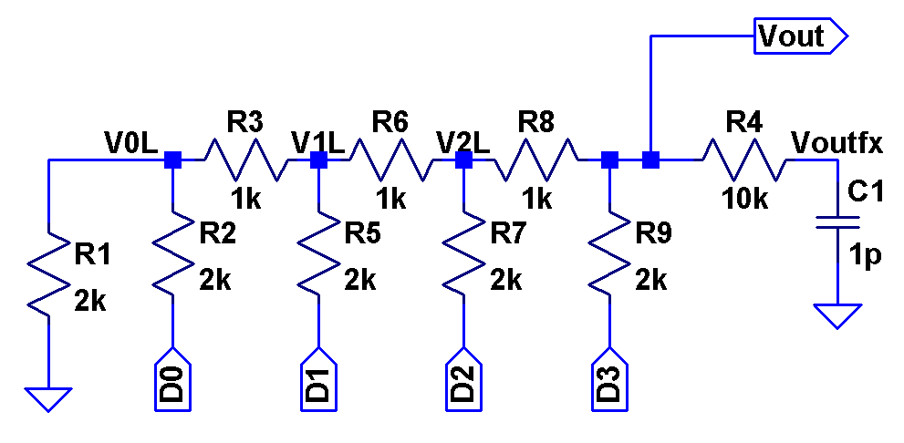
Lab Introduction - ADC DAC Schematic and simulation
In this guided laboratory, our task is to make some simulation and analysis of a ramp and sine signal applied to an electronic circuit that
consists of both ADC and DAC circuits inside, which is designed in LTspice. Our basic expectation is to get an output that is similar to the input,
and then we will see how much deviation we have by using error analysis techniques like DNL, INL, LSB for the ramp and FFT, DNL, INL, SNR for the sine
signal. These will give us clear information for the practical implementation of the ADC DAC circuit, and we will see whether the behavior is the same
or not.
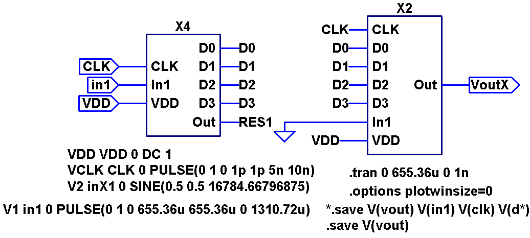
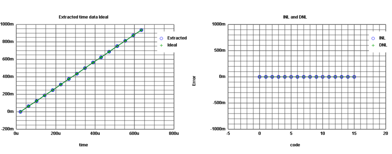
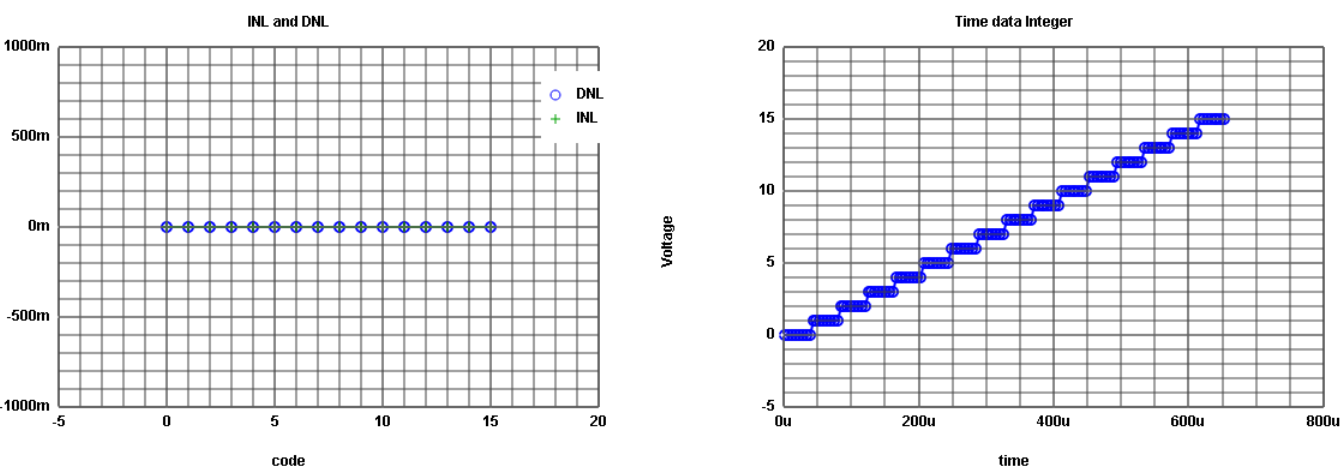
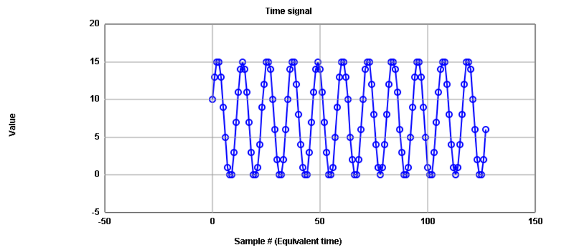
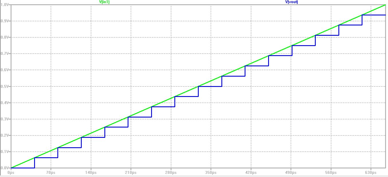
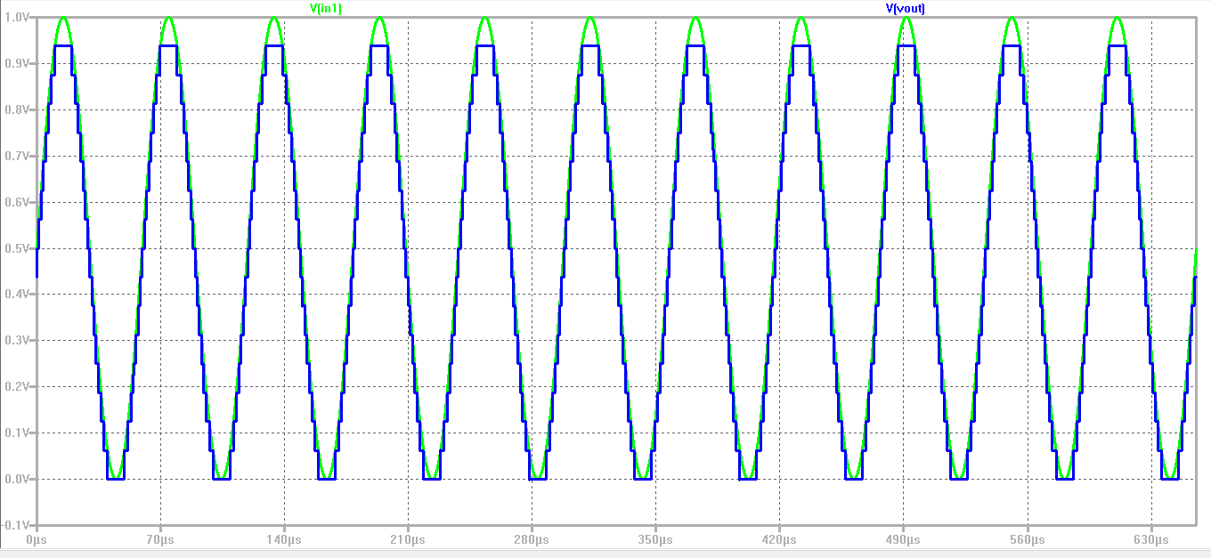
The ADC-DAC circuit is shown in the above figure. So by using the voltage V1 or V2, we can do the ramp and sine signal test in LTspice. The result
of this simulation is shown below. In both inputs, the input signal is a smooth analog signal and the output is a kind of staircase because of the
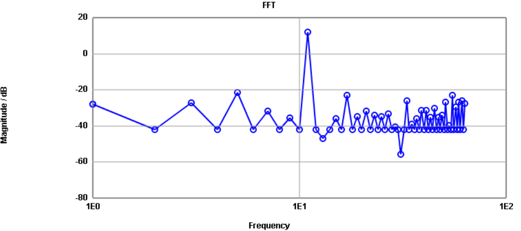
discretization. We have also an FFT simulation option in LTspice and from that, we were abe to see the signal to noise ratio of the input signal
but we couldn't see the SNR of the output due to the case that LTspice doesn’t provide us with all the values for our data converter analysis.
FFT of the input and output of the sine signal from LTspice.

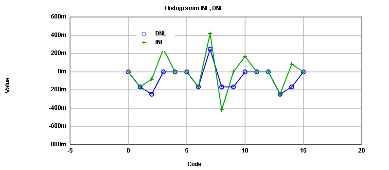
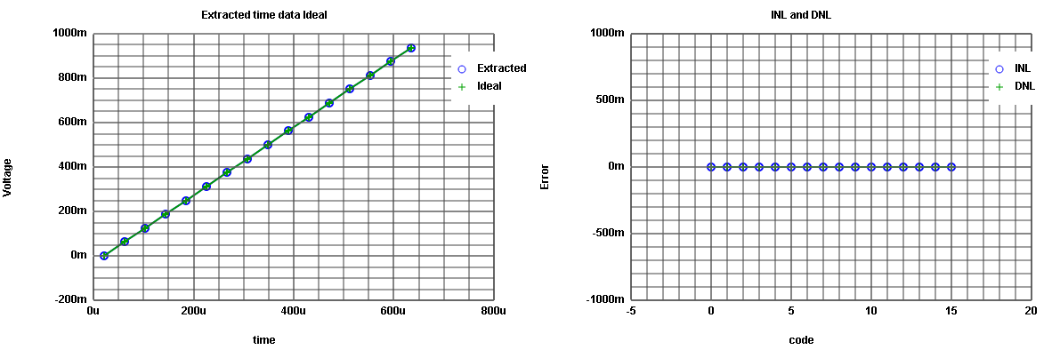
Simulation R2R DAC
Now we have replaced our DAC converter to R2R circuit and after simulation the ideal output is as shown below.
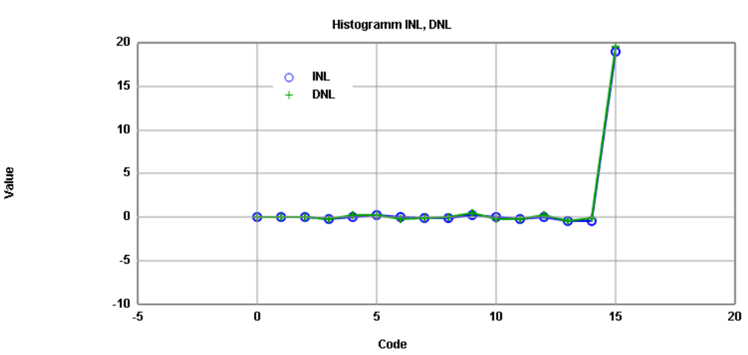
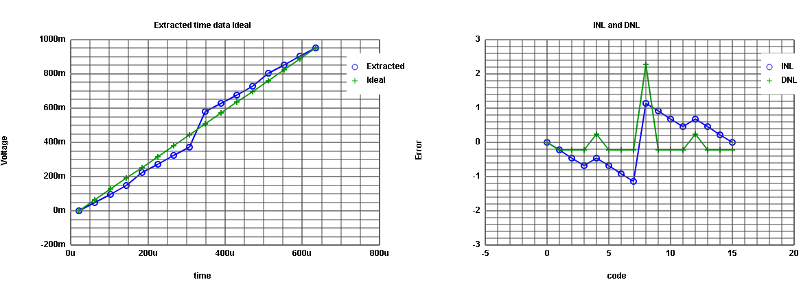
For further investigation, we have changed the resistance R6 to 1.3k and R9 to 1.5k. Then from the figure below we can see how much
our output curve and DNL, INL are changed. In order to see the effect, we made a big change in the resistance. The change in the resistance
could be due to temperature. In reality, there is no significant change. But even though the change is small it can be easily detected by
the INL DNL simulation. The result of this new resistance value is shown here. We can see the big jump in the middle (due to the highest
order bit resistance change’ R9’) and the two terms of the lower order bit on the right and left (due to R6).
Learning Outcomes and Challenges
From this lab, I understand more details on how to convert an analog signal to a digital signal and vice versa. I learn how we can take samples
and what possible errors can occur. Then by applying a ramp and sine signals, I have learned how I can measure the performance of ADC DAC converter
with DNL, INL, SNR (FFT). Then for real circuit simulation, we consider the R2R DAC circuit, and we also assume that in reality the resistance value
can be changed and this change causes errors but then we successfully detect these errors by the DNL INL test and this can be debugged by adjusting the
values of the resistors.
Moreover, I have also upgraded my knowledge of Webpage editing.
Time Spent
I spent about twelve hours to complete this laboratory. Eight hours to simulate and
understand the concept, 2 hours to write and edit it, and last two hours to put it on a webpage.
|